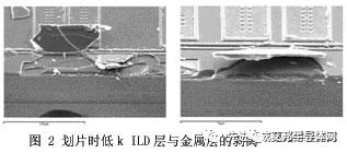
Figure 1 D1, D2 represent the portion of the dicing block that remains intact, and FSC refers to the size of the front collapse. According to the packaging process design rules, the minimum value of D1 and D2 can be 0, and the width of the area where the collapse Angle is allowed is (block width - knife mark width)/2, which is the average value of D1 and D2, and the variance of D1 and D2. According to the statistical principle, for a qualified dicing process, its cutting ability index should be greater than 1.5. Delamination & Peeling Due to the unique material properties of the low ILD layer, the failure mode of low k wafer cutting in addition to the collapse defect, delamination and peeling of the metal layer and ILD layer at the edge of the chip is another major defect (Figure 2).
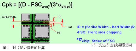
FIG. 2 Delamination and stripping of ILD layer and metal layer at the edge of the chip
For low k wafer cutting quality assessment, in addition to front and back flaring, the following cutting quality indicators are specified based on experimental data and reliability results: (1) The copper seal ring is not allowed to break, delamination or any other visible damage (under a 200x microscope). (2) The delamination of metal and ILD layers on a dicing block is permitted, provided that this delamination stops outside the copper seal ring. (3) The metal/ILD layer in the top corner area of the chip is not allowed to delamination or damage, the only exception is that the package reliability data proves that the damage in the top corner area of the chip is acceptable under a particular combination of chip design/package structure.
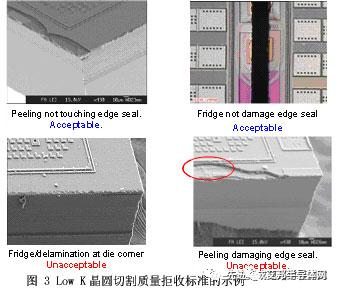
Figure 3 shows an example of the rejection criteria for low k wafer cut quality.
Figure 3 Low k wafer cut quality rejection criteria
The important factors affecting the quality of wafer dicing
dicing tools, materials and dicing parameters
dicing tools and materials include Dicing blade and Mounting tape. dicing parameters include cutting mode and cutting parameters (step speed, blade speed, cutting depth, etc.). For wafers made by different semiconductor processes, it is necessary to select the dicing tools and optimize the parameters to achieve the best cutting quality and the lowest cutting cost.
Test patterns for cutting blocks
In the wafer manufacturing process, in order to obtain a high yield, low manufacturing costs and stable process, each step of the process is under strict monitoring. Therefore, the test pattern was designed and monitored to ensure that key parameters such as electrical parameters, process accuracy such as ILD/metal deposition thickness, mask alignment accuracy and wire tolerance met the design requirements. There are generally 3 ways to achieve wafer process monitoring:
(1) Offline test. This test places all the test patterns on a specially designed Wafer called a "Process Validation Wafer". The advantage is that all patterns to be tested can be included, so that a comprehensive process monitoring can be performed; The disadvantage is high cost and time. It is usually used in the early stages of product development. As product technology matures, this test method will be replaced by other test methods.
(2) Test chip insertion method. All the test patterns are put into test chips, which are placed on different areas of the wafer. The number and location of test chips depends on the complexity of wafer fabrication technology. The advantage is that it is a real-time monitoring. If a fatal defect occurs early in the wafer manufacturing process, the loss caused by the entire wafer being scrapped can be avoided. The disadvantage of this test method is that it takes up valuable silicon Wafer resources, especially when the individual chip size is large and the number of PDPW(Potential Die Per Wafer) is small.
(3) Peripheral testing. The test pattern is placed within a slicked block (Figure 4). Placing the test pattern within the slated block enables real-time monitoring while saving valuable wafer resources. The number of test patterns that can be put into the sliced blocks depends on the length and area of the sliced blocks in a mask (Reticle). Test patterns on a Reticle block are replicated across the entire wafer as step lithography progresses. Within Reticle, all test patterns are unique and distinct from each other. Between Reticle and Reticle, the test pattern is repeated.
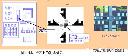
FIG. 4 The test pattern is placed within the slicked block
Optimization of wafer dicing process
A new type of slice quality evaluation matrix
In order to evaluate the quality of wafer cutting, it is essential to inspect the wafer with an optical microscope after the dicing process. In order to gain an understanding of the overall cut quality, it is critical to develop a reasonable sampling plan, including sampling location and sample number. In the traditional sampling plan, the chip to be inspected is selected near the edge of the wafer, and one chip is picked up in each of the 8 directions of the clock hands, such as 1, 3, 5, 6, 7, 9, 11, and 12 for chip defect inspection. This inspection method is suitable for mature non-low-K wafers. However, when applied to low-K wafers, it no longer provides a comprehensive picture of cut quality.
The main reason for the above results is that there are more cutting defects in low-K wafers, and they are different from those in non-low-K wafers. Application of traditional inspection methods for different wafers, the obtained inspection results are very different, and different inspectors on the same wafer inspection results are not the same. The reason for this is that, on the one hand, different inspectors use random inspection methods, which is difficult to obtain a comprehensive assessment of the cutting quality of low-K wafers, and it is difficult to detect the most serious cases. The main reason is that the inspection method does not take into account the structure and distribution of the test pattern on the chip, and the structure and distribution of the test pattern are closely related to the wafer manufacturing process and process control method.
Usually the dicing process/equipment is stable, and the cutting quality is largely related to the structure of the dicing block, such as the test pattern on the block, the material properties of the metal layer versus the ILD layer. The data show that for blocks in different Reticle but with the same position/same test pattern within Reticle, the cutting quality is very close or even exactly the same. Thus, by checking the cutting quality of all blocks within a Reticle, the cutting quality of the entire wafer can be known. In other words, it is impossible to obtain a comprehensive understanding of the cutting quality of the entire wafer without 100% cutting quality inspection of a Reticle, which is the reason for the deviation of traditional dicing quality inspection methods.
The number of chips that a Reticle can hold varies with the chip size and the lithographic accuracy required. For a 12-inch wafer with 90nm technology and a chip size of 6x6mm2, a Reticle can accommodate 20 chips. This test method is more than 98% more efficient than 100% full inspection, and the inspection workload is only 2% of the full inspection, thus solving the operability of the dicing inspection.
Based on the above discussion, the low-K slice quality evaluation matrix is designed (Figure 5), which can also be used to evaluate the cut quality of non-low-K wafers.
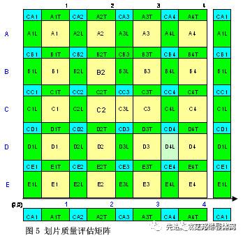
FIG. 5 Low k slice quality evaluation matrix
A Reticle is removed from the wafer, with the English letters A, B, C... To represent the line number of the chip in Reticle, and the numbers 1, 2, 3... The column number that represents the position of the chip in Reticle, and each chip can be uniquely identified in a Reticle. Such as A1, B3 and so on. There are 4 edges and 4 vertices around each chip. If A1T(A1 Top) represents the block above the A1 chip, A1L(A1 Left) represents the block to the left of the A1 chip, and CA1(Corner A1) represents the block crossing section at the top left of the A1 chip. In this way, the cutting quality of the entire wafer can be clearly expressed through the cutting status of XT, XL, CX (X represents the coordinates of the chip) in a Reticle. Another advantage of this quality evaluation matrix is that it is easy to find a chip with a specific test pattern on the wafer and observe its cutting quality. A test pattern and its cutting quality can also be analyzed or improved offline. Before that, it takes experience and skill to identify a Reticle.
Blade selection and optimization
The cutting knife, also known as the diamond cutting knife, contains three main elements: the size, density and bonding material of the diamond particles. Diamond particles act as an abrasive in the wafer cutting process and are usually synthesized from CBN(Cubic Boron Nitride). Diamond particle size varies from 2um to 8um. In order to achieve better cutting quality, diamond particles with edges are usually selected. The density of diamond particles represents the volume ratio of diamond particles to diamond blades. Generally, blade suppliers will provide different diamond particle densities to adapt to different applications. The metal nickel is used as a binder to bond the diamond particles together.
The choice of cutting knife generally takes into account cutting quality, cutting blade life and production costs. Diamond particle size affects the life and cutting quality of the blade. Larger diamond granularity can grind away more silicon material at the same tool speed, so the life of the tool can be extended. However, it reduces the quality of the cut (especially front flanging and metal/ILD delamination). Therefore, the choice of diamond particle size should take into account cutting quality and manufacturing costs.
The density of diamond particles is also critical to the control of cutting quality. For blades of the same diamond particle size but with different densities, the amount of silicon material removed by the blade per rotation cycle is the same, but the average amount of silicon material removed to each diamond particle is different.
It is found that the high density of diamond particles can prolong the life of the blade and reduce the back of the wafer. And low density diamond particles can reduce the front crack. Hard bonding materials can better "fix" diamond particles, which can improve the life of the blade, while soft bonding materials can accelerate the "Self Sharpening" effect of diamond particles, so that diamond particles maintain sharp angular shape, which can reduce the front of the wafer crash or delamination. But the cost is the shortening of the life of the blade. The length of the blade should be defined according to the thickness of the wafer, the thickness of the carrying film, and the size of the maximum allowable breakage, and the blade should not be chosen too long, because the long blade will cause the blade to swing when cutting, which will lead to a larger breakage.
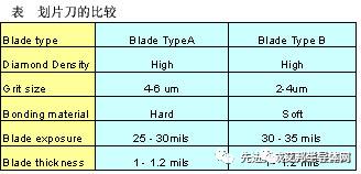
For low k wafers, the delamination or stripping of the metal/ILD layer and the collapse of the Angle are more important than the production cost (to the extent permitted by the production cost). Based on the experiment, the dicing knife with 2-4um diamond particle, lower diamond density and softer binder material is selected as the basis for further optimization of dicing process. Figure 6 is a comparison of the cutting quality of different types of dicing knives. dicing knife A has A larger diamond particle, a harder bonding material, and dicing knife B has a smaller diamond particle, a softer bonding material (table), it is obvious that the cutting quality of dicing knife B is better than dicing knife A.
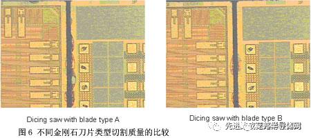
FIG. 6 Comparison of cutting quality of different types of dicing knives
Mounting Tape is attached to the back of the wafer before dicing. It is used to keep the separated chips attached to the wafer after dicing so that the Die Bonder can complete the dicing process. The viscosity of the film is an important property for the quality of the dicing. Experiments show that higher bonding force between thin film and silicon wafer can effectively reduce the crack on the back of wafer.
On the other hand, in the adhesive film process, it is hoped that the adhesive force between the film and the silicon wafer is as small as possible, so that the adhesive film process can obtain a robust process window to avoid potential chip breakage and production efficiency problems caused by too high Ejector Pin setting or too long Pick Up Time setting. In order to take into account the two processes of dicing and gluing, ultraviolet photosensitive film (UV Tape) is selected as the bearer film of the wafer. A notable feature of the UV film is that its adhesion to the silicon wafer is very high before ultraviolet light irradiation, up to 16000mN/25mm, and after ultraviolet light irradiation, the adhesion decreases significantly, up to 600mN/25mm. The bond strength changed 25 times before and after UV irradiation. This property of UV film is very compatible with the quality control of dicing and sticking.
The choice of dicing mode
The dicing machine generally provides two cutting modes, Single Cut and Step Cut, the difference between them is shown in Figure 7. The experiment proves that the design of dicing knife cannot meet the quality control requirements of front Angle breakage, lamination and back Angle breakage at the same time. This conclusion is especially applicable for low-K wafers with wafer thickness greater than 7 mil. In order to reduce the delamination between the front metal layer and the ILD layer, the thin blade is preferred, and if the wafer is thicker, the blade with a longer blade should be selected. However, it should be noted that the blade with a higher blade/blade width ratio will swing when cutting, but will cause a larger front delamination and back collapse.
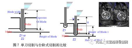
Figure 7 The difference between single-knife cutting and bench cutting
The stepped cutting uses two dicing knives, the first is thicker and is programmed to cut into the wafer at a certain depth, and the second is thinner and cuts through the entire wafer along the center of the first dicing knife cut and carries the film down to 1/3 of the thickness. The advantages of bench cutting are: reducing the pressure of the blade on the wafer during the cutting process; Reduce the mechanical wobble and serious corner breakage caused by the need to use a higher blade height/blade width ratio; Provides the possibility to select different types of dicing tools to optimize the front dicing/lamination and back dicing respectively.
Additives for dicing cooling water
Adding some chemical additives to the cooling water of the dicing machine can effectively reduce the surface tension of the DI water on the wafer/dicing knife, thus eliminating the accumulation of silicon chips and metal particles generated by wafer cutting on the wafer surface and the surface of the dicing knife, cleaning the chip surface, and reducing the back of the chip. The accumulation of these silicon chips and metal chips is a major cause of Bonding Pad contamination and wafer back breakage. Therefore, when optimizing the dicing knife and dicing parameters cannot eliminate the chip back collapse, additives for dicing cooling water can be considered.
Optimization of dicing process parameters
After determining the design and selection of the dicing knife, the bearing film and the cutting mode, the next step is to further reduce the dicing defects of low-K wafers by optimizing the dicing process parameters. Based on the previous experimental results and the screening of the dicing process parameters, three important process parameters were selected for process optimization, including the dicing tool speed, the bench stepping speed and the cutting depth of the first dicing tool. One of the difficulties in the optimization of low k cutting process is to determine the response of experimental design. Different metrics had been considered, including measuring the size of the metal /IL stripping in vertical and parallel directions to the cut block (a, b1, b2 see Figure 8), or measuring the length of the stripping area as a percentage of the length of the fixed block, but statistical analysis of the data measured according to these metrics found that even for the same set of parameter Settings, There is also a large variation, so it can not be used to optimize the low k cutting process.
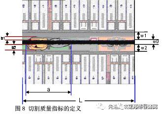
FIG. 8 Determination of response index of experimental design for low-K cutting process optimization
Finally, it is found that the ratio of the area of the calculated area with cutting defects (S1-S2) to the area of the fixed area (S3-S2) (S1-S2/S3-S2) can accurately reflect the difference of cutting quality under different cutting parameters. In FIG. 8, the area S that allows dicing to produce defects is a figure surrounded by W1, L, W2 and L. Since the dicing part of the block cut by the dicing knife will be deformed due to the tension of the bearing film after dicing, (w1+w0+w2) is not equal to the width of the block, so W1, L and W2 and L need to be calculated separately. However, the dicing defect area (S1) surrounded by b1, a, b2 and a cannot be calculated directly through linear size calculation. Photoshop is used to draw the contour line of the defect area, and the defect pattern is converted into binary black and white pattern by pixel filling and reverse display. Finally, the number of black pixels in the fixed area is calculated. The percentage of (S1-S2) /(S3-S2) is obtained to obtain the corresponding data of the experimental design. Figure 9 shows the method for determining the graph area of the defect area.
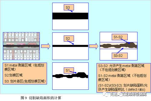
Figure 9. Method for determining the graphic area of the defect area
Improvements to test patterns on dicing blocks
Although the delamination and stripping of the metal layer/ILD were strictly controlled outside the copper seal ring through process optimization, the delamination/stripping phenomenon was not completely eliminated. Moreover, the impact of this delamination/stripping on the reliability of other semiconductor packaging forms (such as Flip Chip) still needs to be verified with relevant reliability data. It is therefore necessary to continue researching solutions that completely eliminate metal/ILD delamination/stripping.
First of all, cooperation between the chip design/manufacturing plant and the packaging plant is required. Experiments have found that some severe ILD delamination/stripping of metal always occurs on a few blocks containing specific test patterns. In some blocks that do not contain test patterns, the defects of layering and stripping are almost zero. One implication here is that chip factories can modify the test pattern to make it resistant to the delamination/stripping that occurs in the dicing process. For example, by adding a virtual "L" pattern to the test pattern of the dicing blocks, the layering and stripping of heavy metal/ILD layers is almost eliminated.
In addition, within a limited block width (such as 120um), if the test pattern can be limited to 70um and placed on one side of the block, then on the other side of the block, a 50um wide "blank" area is formed. If this 50um wide area is taken as an imaginary block, the dicing of a low-K wafer becomes a dicing problem for a narrow (50um) non-low-K wafer (Figure 10). According to the current dicing machine and dicing process capability, this cutting method is feasible.
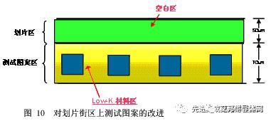
FIG. 10 Cutting methods feasible with current dicing machine and dicing process capability
In addition, not all test patterns are necessary for the process inspection of the chip factory. The test pattern exists in the form of a modular (Mask Set). Sometimes, the production inspection of a certain IC manufacturing process requires certain test patterns from several modules, and the lithography engineer often does not remove the useless test patterns after selecting the module where the required test patterns are located. The result of this is to increase the complexity of low-K wafer dicing process and reduce the dicing process window. It shows that in order to ensure the economical scale production and reliability of low-K semiconductor products, the industry needs to consider and optimize the pre-process and post-process as a whole, so as to avoid the emergence of "bottleneck" processes as much as possible.
The laser cutting industry is also trying to find an alternative to the mechanical dicing of low-K wafers, and laser cutting is one of them. Strictly speaking, the laser beam does not "cut" the low k layer, but relies on the high temperature melting metal layer/ILD layer generated by the laser energy. This laser cutting creates very little mechanical stress on the metal/ILD layer, so there is no problem of delamination or stripping of the metal/ILD layer, because the mechanical dicing machine no longer cuts the low k layer. At present, laserdicing saw have begun to be used in the dicing process of low-K wafers of 65 nm and below. However, the high cost of equipment is still a major reason restricting the popularity of laserdicing saw.
Sum up
In this paper, the working principle of the dicing machine, the main defects of the dicing process and the traditional dicing quality evaluation method are introduced. On this basis, a new method, the matrix of wafer cutting quality evaluation, is proposed, which can analyze and evaluate the cutting quality comprehensively and objectively. This chapter also defines the main characteristics of the cutting quality assessment, discusses the main factors affecting the cutting quality of low k wafers and optimizes the process parameters of low k wafers by using the experimental design method. At the same time, attempts and efforts are made to cooperate with chip factories to further improve the cutting quality of low-K wafers, and a feasible scheme is put forward. Finally, a new type of non-mechanical dicing machine - laser dicing machine is briefly introduced.
(Article from wechat public number: Semiconductor materials and process equipment)