Mention "semiconductor", we may come to mind is the esoteric and remote concept of science and technology. However, in fact, it has been everywhere, integrated into our lives: from the smart phone in the hand to the laptop on the desk, these indispensable items in daily life, behind the semiconductor support.
This paper will focus on the semiconductor packaging industry. Semiconductor encapsulation is a process in which wafers qualified for testing are packaged and detected to obtain independent chips after wafer design and manufacturing is completed. It includes packaging and testing two main links, of which packaging is to process the chip into an independent form according to the product model and functional requirements, and testing is to test the performance and quality of the packaged chip. Semiconductor encapsulation is the last step in the semiconductor production process and is critical to ensuring the performance and quality of the chip. With the continuous development of the semiconductor industry, packaging technology is also constantly improving and has undergone many major innovations.
The basic process of semiconductor encapsulation roughly includes the following steps:
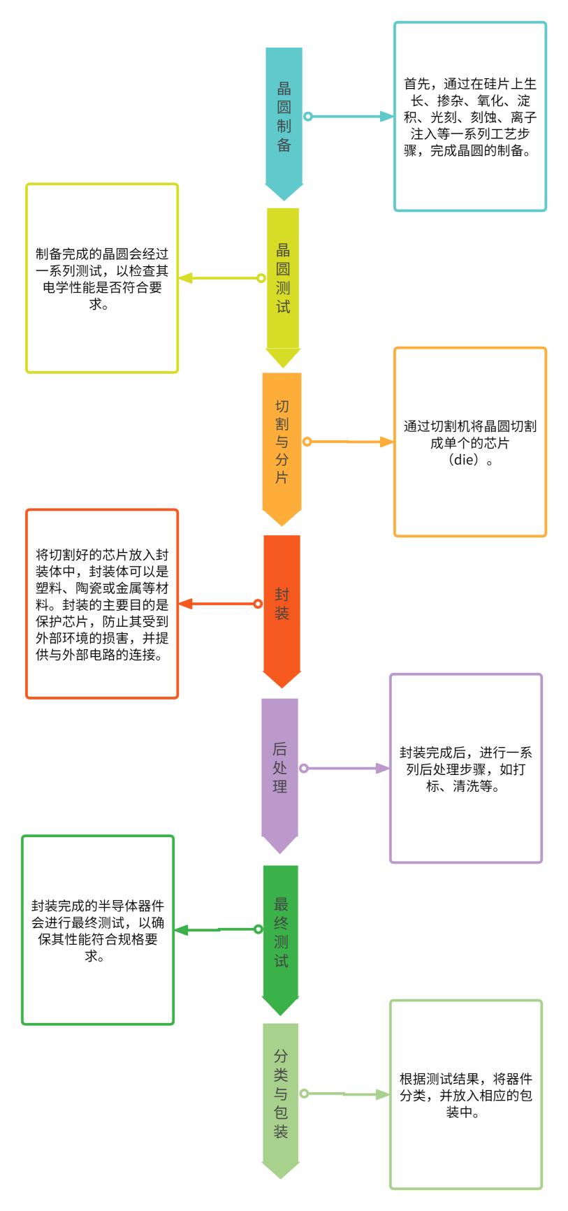
The above is a simplified process, the actual semiconductor sealing process can vary depending on the product type, package type, and manufacturer's process differences, and also derived a lot of technical terms. Next, this article will focus on three of the key processes.
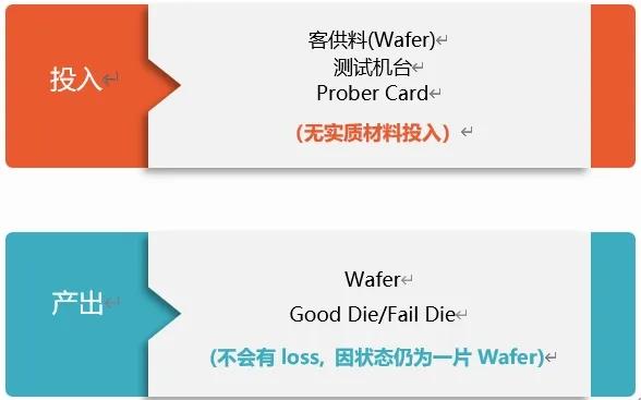
The first is the CP test. CP (Chip Probing) refers to wafer testing, between wafer fabrication and packaging in the entire chip making process. After the Wafer is made, thousands of naked dies (unpackaged chips) are regularly distributed throughout the Wafer. Since the chip has not been sliced and packaged, the pins of the chip are all exposed, and these extremely small pins need to be connected to the Tester through a thinner Probe.
Why do CP tests? This is because, in the semiconductor manufacturing process, after the Wafer production is completed, due to the complexity of the production process and the influence of various factors, a certain number of manufacturing defects will inevitably appear in the bare DIE. These defects can cause chip performance degradation or function failure. The main purpose of CP test is to comprehensively detect the naked DIE on Wafer to identify and eliminate those defective products with manufacturing defects. Through this process, we can significantly increase the rate of good products leaving the factory, thereby reducing the cost of subsequent packaging and testing. This not only helps improve overall production efficiency, but also provides customers with more reliable products. In addition, during the chip packaging process, some pins may be encapsulated internally, resulting in the function of these pins cannot be tested after packaging.
Therefore, the CP test is the only opportunity to assess the normality of these functions. With CP testing, we can ensure that all critical functions meet expectations before packaging, thus avoiding potential performance issues. In addition, some advanced semiconductor companies will also grade the performance of the chip according to the results of CP testing. This means that they will classify chips into different grades based on their performance differences, and put these products in different markets. This strategy helps meet the needs of different customers and creates greater market value for the company.
The second important process is Assembly. Common packaging forms are:
Single-in-line Package (SIP)
Dual in-line Package (DIP)
Thin Compact Package (TSOP)
Plastic Square Flat Package (QFP) and Plastic Flat Component Package (PFP)
Pin Grid Array (PGA)
Zigzag in-line Package (ZIP)
Ball Grid Array Package (BGA)
Planar Grid Array Package (LGA)
Plastic Electrode Wafer Carrier (PLCC)
Surface Mount Device (SMD)
Pin-less Chip Carrier (LCC)
Multichip Module (MCM)
The following figure illustrates the main points of an Assembly process:
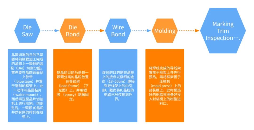
In this process, it should be noted that the Wafer is converted to Die, and its unit is also converted from PCS to EA. More attention should be paid to the packaging form than the finished product.
The third is the FT Test, also known as Final Test, is an important part of the semiconductor industry, mainly for the final performance and functional testing of the packaged chip.
In FT TEST, the test device connects to the pin of the chip and evaluates the performance and functional effectiveness of the chip under different operating conditions by applying test commands and collecting output signals. These tests are designed to ensure that the chip can meet the expected performance standards in practical applications, and has stability and reliability. FT TEST usually includes many aspects such as electrical performance test and functional verification. Electrical performance testing focuses on the electrical characteristics of the chip, such as voltage, current, resistance, capacitance, etc., to ensure that they meet the design requirements. Functional verification focuses on whether the functions of the chip work normally according to the design requirements, including logic function testing, interface testing, etc.
In addition, FT TEST also involves environmental testing and reliability testing of the chip to evaluate the performance and stability of the chip under different environmental conditions. Environmental testing may include testing under high temperature, low temperature, humidity, vibration and other conditions to ensure that the chip can work properly in a variety of practical use environments. Reliability testing focuses on the life and long-term stability of the chip, and evaluates the reliability of the chip through long-term aging test and temperature cycle test.
FT TEST is the last hurdle to ensure the quality of semiconductor products, and only chips that pass this test will be shipped. Therefore, FT TEST is essential to ensure the performance and reliability of semiconductor components. At the same time, as semiconductor technology continues to evolve, FT TEST continues to evolve and improve to meet the needs of more complex and rigorous testing.
Among them, the number of tests and test procedures are often determined by the customer.
In addition to the above processes, there are other important terms and concepts in the semiconductor packaging industry that are also important for understanding industry operations and processes. For example:
Wafer bumping, that is, Wafer bumps, is essential for flip chip or Wafer Level Chip Scale Package (WLCSP). Bumping is an advanced wafer-level process technology in which "Bumps" or "Balls" made of solder are formed on a Wafer in the form of an entire wafer before the wafer is cut into a single chip. These "bulks" can consist of eutectic, lead-free, high-lead materials, or Cu pillars on wafers, which are the basic interconnecting components that interconnect the chip (die) and substrate together to form a single package.
COF:Chip on Film. Thin-film encapsulation is the use of flexible printed circuit film as the carrier of encapsulated wafers. The technique of Bonding the Gold Bump on the wafer to the Inner Lead on the circuit of the soft substrate by hot pressing.
COG:Chip on Glass. It is an advanced packaging technology that connects the IC with the glass substrate. After the LCD Panel module factory obtains the driver IC, Flip Chip technology is used to engage the Bump on the driver IC and the ITO endpoint on the LCD panel with ACF Conductive Film (full name of Anisotropic Conductive Film) as the intermediate interface. Mainly used in liquid crystal display driver IC package.
.....
It can be seen that the birth of a semiconductor product contains the interweaving of hundreds of precise processes. The complexity of its process is mainly reflected in the following points:
Fine process flow: Semiconductor sealing involves a number of fine process flow, such as chip cutting, thinning, mounting, welding, packaging, testing and so on. Each step requires precise control of various parameters, such as temperature, pressure, time, etc., to ensure the performance and reliability of the chip. For example, in the cutting process, high-precision cutting equipment is needed to cut the wafer into individual chips, which requires extremely high cutting precision to avoid damaging the chip or affecting its performance.
Strict quality requirements: The semiconductor packaging industry is extremely strict about the quality of products, because any small defect can cause chip performance degradation or failure. Therefore, it is necessary to carry out multiple quality inspection and control in the process, such as appearance inspection, electrical performance testing, etc., to ensure that each chip meets the specifications.
Highly automated production lines: Due to the complexity and quality requirements of the semiconductor sealing process, production lines usually employ highly automated equipment and systems. These devices and systems need to have high precision, high stability and high reliability to ensure process stability and consistency. For example, an automated chip mounter can quickly and accurately mount the chip to the substrate, and an automated test device can perform a comprehensive electrical performance test on the chip.
Clean production environment: Semiconductor seal testing needs to be carried out in a highly clean environment to avoid the impact of dust, particulate matter and other pollution on the product. Therefore, the production line is usually built in a clean room, and uses a variety of air purification technologies, such as high-efficiency filtration, laminar air supply, etc., to ensure the cleanliness of the production environment.
I believe that the astute consultants have also noticed that these characteristics pose many challenges to the implementation of SAP projects, including:
The complexity of data processing: the semiconductor sealing process involves a large amount of data, including equipment parameters, process flow, quality test results, product traceability information, etc. These data need to be processed accurately and efficiently in the SAP system to support the production management and quality control of the enterprise. However, due to the complexity of the process, the collection, integration and analysis of data became extremely difficult, requiring deep industry knowledge and technical background of SAP consultants.
Business process customization needs: The business process of semiconductor sealing enterprises often has a high degree of customization needs, because different enterprises' products, equipment, processes, etc., are different. This makes the implementation of SAP systems require a lot of customized configuration and development work to meet the special needs of the enterprise. Consultants need to have a deep understanding of the business process and process characteristics of the enterprise to provide targeted solutions.
Quality control and traceability challenges: The semiconductor packaging industry has extremely high requirements for product quality, making SAP systems need to play a strong quality management and traceability function, which can support enterprises to conduct comprehensive quality monitoring and traceability of products. This is also a major difficulty in the implementation process.
The challenge of integration and collaboration: The supply chain of the semiconductor packaging industry involves multiple links and multiple enterprises, such as raw material suppliers, equipment manufacturers, logistics companies, etc. SAP systems need to integrate and collaborate with these external systems to ensure data sharing and smooth business processes. However, due to the special nature of the semiconductor industry, these integrations and collaborative work often face many challenges, such as inconsistent data formats and incompatible system interfaces.
Indeed, the implementation of SAP projects related to the semiconductor industry is challenging due to its professionalism and complexity, which is no doubt no small test for consultants. However, no matter which industry you are in, it is a task that we should pay attention to to continuously improve our professional quality and skill level. Only in this way, in the face of endless challenges and constantly updated technology, can maintain a keen insight and adaptability, so as to better adapt to and cope with new situations and new problems. This is essential to our professional growth and the key to delivering exceptional service to our clients.
(Article transferred from wechat public number: Memory fragments of Love remember not remember, author: Yao Jingxian)